Researchers from the Institute of Technical Physics and Materials Science of the HUN-REN Centre for Energy Research (HUN-REN EK MFA) participated in an international collaboration in the development of Qubits, which form the basis of quantum computers. During the project, they developed a JoFET Qubit that is compatible with silicon-based manufacturing processes, so it will be easier to upscale in production. The researchers used modern, new types of materials and developed characterization processes for TEM, which enabled the production of the necessary superconducting layers.
Researchers from the Institute of Technical Physics and Materials Science of the HUN-REN Centre for Energy Research (HUN-REN EK MFA) have been participating in the SIQUOS project, a consortium with the Centre for Nanosciences and Nanotechnologies (C2N) and Uppsala University, for the past three years, in the development of Qubits, the basis of quantum computers. The results of the SIQUOS project bring us one step closer to the realization of scalable – i.e. mass-produced – Qubits based on existing advanced silicon technology. Qubits are the basic building blocks of quantum technology devices and will play a role in both the development of quantum computers and the implementation of new types of sensors.
Among the various technologies used to implement Qubits, the most advanced is the solid-state electronic solution using superconductors. These are usually based on a Josephson junction (JJ) with a weak coupling between two superconducting contacts. One type of current Qubit, the transmon (JJs are based on a tunnel junction solution), is difficult to scale and generates enormous heat in large masses. Therefore, a new solution, the gatemon (in which JJs are replaced by a single gate-controlled, superconducting/semiconductor hybrid nanostructure JJ), has come to the fore, which is better suited to modern semiconductor technologies. A special version of the latter is the JoFET, where there is good electrical transparency between the semiconductor source and drain (S&D) contacts and the semiconductor channel and the gate length is sufficiently short, and a non-dissipative superconducting current flows in the device, the amplitude of which can be controlled by the electrostatic gate.
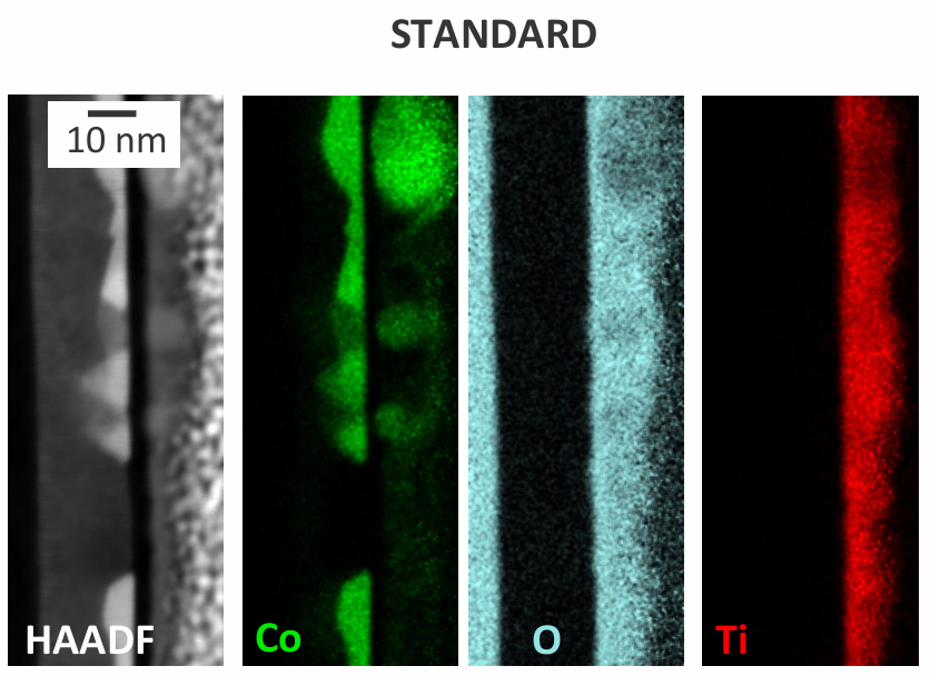
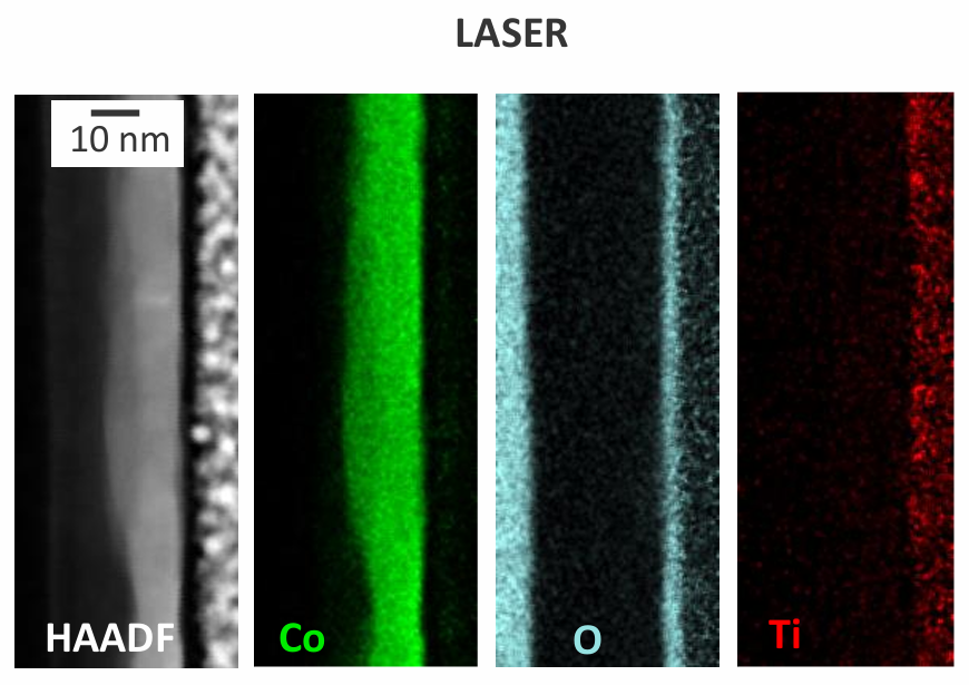
The primary result of the SIQUOS project is that the transistor structures required for JoFET were created exclusively with materials compatible with existing Si technology (PtSi, CoSi2 and heavily boron-doped silicon (Si:B)), so that up scalable manufacturing of devices is easier achievable.
To create the thin superconducting layers required for the transistor’s S&D contacts and to reduce the Schottky barrier of the Si/PtSi interface, it was necessary to develop new (but compatible with existing technologies) technological steps. In the case of the CoSi2 superconducting contact, the formation of the desired quality Si/CoSi2 interface also required a modification of the heat treatment step. The technology development of the French and Swedish partners was assisted by the atomic-level structural investigation of the HUN-REN EK MFA, in which the country’s only aberration corrected electron microscope played a major role. During the project, the existing characterization technological procedures were expanded with their own methodological, electron diffraction developments. This also proved that such high-tech semiconductor developments cannot be followed without high-resolution electron microscopy.
The SIQUOS project (grant no. 2019-2.1.7-ERA-NET-2022-00032) was supported by the National Research, Development and Innovation Fund.
More information:
Dr. János Lábár, project leader, labar.janos@ek.hun-ren.hu